| Magazines: AutoSpeed | Rallysport | V8X | Silicon Chip | Shopping: Property | Cars | Fishing |
 |
| Current Articles | | | Archived Articles | | | Search | | | Free Preview | | | Register |

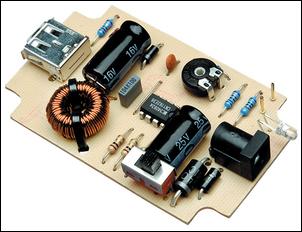
Using the USB port on your computer to charge your player’s batteries is not always practical. What if you do not have a computer available at the time or if you do not want to power up a computer just for charging? Or what if you are travelling? Chargers for iPODs and MP3 players are available but they are expensive and you need separate models for charging at home and in the car. SILICON CHIP’s new charger can be used virtually anywhere. While we call the unit a charger, it really is nothing more than a 5V supply that has a USB outlet. The actual charging circuit is incorporated within the iPOD or MP3 player itself, which only requires a 5V supply. As well as charging, this supply can run USB-powered accessories such as reading lights, fans and chargers, particularly for mobile phones. The supply is housed in a small plastic case with a DC input socket at one end and a USB type "A" outlet at the other end, for connecting to an iPOD or MP3 player when charging. A LED shows when power is available at the USB socket. Maximum current output is 660mA, more than adequate to run any USB-powered accessory. (The specification for the computer USB 2.0 port requires the USB port to deliver up to 500mA at an output voltage between 5.25V and 4.375V).
Circuit detailsThe circuit is based around an MC34063 switchmode regulator. This has high efficiency so that there is very little heat produced inside the box, even when delivering its maximum output current. The circuit is more complicated than if we used a 7805 3-terminal regulator but since the input voltage could be 15V DC or more, the voltage dissipation in such a regulator could be 5W or more at 500mA. and 5W is far too much for a 7805, even with quite a large heatsink. 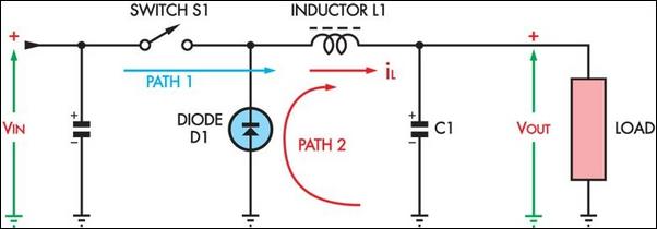
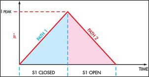
Fig.1(a): the basic scheme for a switchmode power supply. Voltage regulation is achieved by rapidly switching S1.
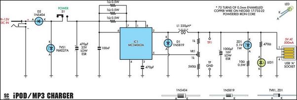
Hence, we have taken the switchmode approach. This is illustrated in Fig.1(a) and involves a switch (S1), inductor L1, diode D1 and capacitor C1. When the switch is closed, current flows through inductor L1 into the load. The current (Path 1) slowly builds up from zero to the peak value, as shown in Fig.1(b). When this peak current is reached, the switch opens and current from the inductor flows through diode D1 to discharge the inductor energy into the load. This current path is shown as Path 2. Capacitor C1 is included to act as a reservoir of power to smooth out the voltage produced across the load. The output voltage is dependent on the load and the ratio of time that switch 1 is closed to when it is open. It is also dependent on the peak current through L1 and the input voltage. This type of circuit can be very efficient because voltage control is achieved by rapidly switching the input. The small amount of power dissipated is mainly due to voltage losses in the switching device and diode D1. Fig.2 shows the full supply circuit, which is based on an MC34063 switchmode controller IC. Its internal schematic is shown in Fig.3. The switching function of S1 [in Fig.1(a)] is provided by the internal transistor (Q1). The internal oscillator sets the switching period, while the "Ipeak sense" limits the current flowing in inductor L1 by controlling the on-time for transistor Q1. The 1.25V reference and comparator provide a feedback arrangement to monitor and control the output voltage. Power from the DC socket passes through diode D2 and slide switch S1 to IC1. D2 protects against reverse polarity and the adjacent Trans-ient Voltage Suppressor (TVS1) clamps any fast spikes which may be riding on the input supply. Further filtering is provided by a 470mF low-ESR (Effective Series Resistance) capacitor. As previously described, current is switched to L1 using the internal transistor in IC1. In operation, the three paralleled 1W resistors between pins 6 & 7 monitor the current through L1. When the current reaches 1A, pin 7 becomes 300mV lower than pin 6 and the internal transistor switches off. The energy stored in L1 is then dumped into capacitor C1 via Schottky diode D1. The resulting output voltage is filtered using a 1000mF low-ESR capacitor. Output voltage controlPin 5 of IC1 monitors the output via a voltage divider consisting of a 1kW resistor, trimpot VR1 and a 560W resistor to ground. VR1 sets the output voltage to 5V. Zener diode ZD1 and the 10W resistor are included to catch any output overshoot voltages which can occur if the output load is suddenly reduced. As explained, the switching of L1 controls output regulation. If the load is suddenly reduced, the only way IC1 can stop any voltage rise is to prevent any switching of power to L1 and let capacitor C1 drop back to 5V. So, to prevent voltage overshoot, ZD1 begins to conduct when the voltage reaches 5.1V, with the current through it limited by its series 10W resistor. In normal circumstances, when the output voltage is correctly set to 5V, ZD1 will not conduct unless the voltage rises momentarily. However, if VR1 is set so that the output voltage is higher than 5V, ZD1 conducts continuously. Because of this, the range of adjustment for VR1 has been deliberately restricted to limit the output to be no more than 6.5V, under worst-case conditions. 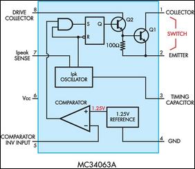
Fig.3:
inside an MC34063 switchmode controller IC. The internal oscillator
sets the switching period, while transistor Q1 does the switching.
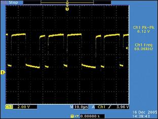
Fig.4:
this switching waveform was measured across the output with an 8Ω
resistive load, resulting in a current of 625mA. Note how the switching
shows signs of "hunting", as the circuit constantly maintains a 5V
output.
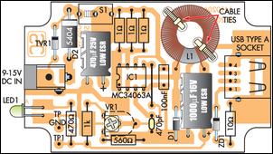
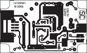
This worst-case setting occurs when VR1 is set fully clockwise (towards the 560W resistor) and when VR1 is 20% high in value and the reference for IC1 is at its maximum at 1.32V (typically, IC1’s reference is 1.25V but this could be anywhere within the range of 1.18V to 1.32V). With 6.5V at the output, there will be 140mA through ZD1 and the 10W resistor. Dissipation in ZD1 will be 0.7W (below its 1W rating), while dissipation in the 10W 0.5W resistor will be 0.2W. When VR1 is set correctly, the output is protected against producing transients above 5V. Should the output become shorted, the fault current will be limited to a safe value at or below 120mA, as set by the paralleled current sense resistors. ConstructionAll the components for the charger are mounted on a PC board coded 14102061 and measuring 79 x 47mm. This board is mounted upside down in a small plastic case measuring 83 x 54 x 31mm.The screw covers for the lid then serve as rubber feet. Begin construction by checking the PC board for breaks or shorts between the copper tracks. Repair these as necessary. That done, make sure the holes are the correct size for each component and check that the PC board clips neatly into the integral side pillars in the box. The component overlay for the PC board is shown in Fig.5. First, insert and solder the resistors, links and trimpot. You should check the resistor values with a digital multimeter. Make sure IC1 is mounted with the orientation shown. The two electrolytic capacitors are mounted on their side to allow clearance in the box; make sure they are mounted with the correct polarity. LED1 is mounted with cranked leads so that it can poke through a hole in the side of the case. Again, take care with its polarity. 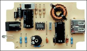
Take
care to ensure that all polarised parts (ie, the IC, diodes and
electrolytic capacitors) are correctly oriented when building the PC
board.
There are four diodes on the PC board, including the zeners and TVS. Make sure you insert the correct ones in each position and with the correct orientation. Once they are in, insert and solder in the two PC stakes followed by slide switch S1. The latter is mounted so that the top of its body is 10mm above the PC board surface. 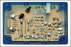
The
PC board is clipped upside down into the bottom of the case and is
secured using an M3 tapped Nylon spacer. This spacer ensures that the
board doesn’t move when the slide switch is operated.
Inductor L1 is wound on a powdered iron toroid with 0.5mm enamelled copper wire. Wind on 75 turns in two layers spaced evenly around the core. The wire ends must be scraped clean of enamel and tinned, before soldering. Alternatively, if the wire is coated with red enamel, this can normally be melted off with the tip of your soldering iron. The toroid is secured to the PC board with two cable ties. These pass through holes in the PC board. Fig.7 shows the drilling details for the case. You have to drill holes for the DC socket and LED in one end, the switch at the top and the USB socket in the other end of the box. Mark these out and drill and file as necessary. TestingInitially wind VR1 fully anticlockwise. That done, set your multimeter to read DC volts and connect it between terminals TP1 and GND. Apply power to the input, switch on and adjust VR1 so that the voltage is 5V. This can generally be set to within 20mV of 5V (ie, 4.98V to 5.02V) using the trimpot. 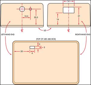
Fig.7:
here are the drilling details for the plastic case. The square cutouts
are made by drilling small holes around the inside perimeter, knocking
out the centre pieces and filing to shape.
Check that LED1 lights. If it doesn’t, check that it is the right way around. If there is still no power indication, use a multimeter to check for voltage at pin 6 of IC1 and for a similar voltage at pins 1, 7 & 8. If there is no voltage here, perhaps the DC socket plug has the wrong polarity. The plug should have the positive to the centre hole and the negative to the outer case. When testing is complete, the PC board can be clipped into the case, making sure the LED protrudes from its hole in the side of the case. The section of PC board directly below the switch will need supporting so it is not pushed out of position when the slide switch is operated. We used an M3 tapped Nylon spacer in the side of the case to support the PC board and this is secured using an M3 screw. To do this hold the spacer tightly against the PC board directly below the switch and mark out the position of the hole for the screw. The transparent box makes positioning of this hole easy. Now drill out the hole and secure the spacer. Finally, fit the lid and insert the rubber feet into the screw holes. Footnote: iPod is a trademark of Apple Computer, Inc.
|
|||||||||||||||||||||||||||||||||||||||||||||||||||||||||||||||||||
|
|
|||||||||||||||||||||||||||||||||||||||||||||||||||||||||||||||||||
|
